How can this chip-based device achieve 1x32 or even more channels of spectral splitting?
The core reason why PLC (Planar Lightwave Circuit) splitters can achieve 1 \times 32, 1 \times 64, or even higher channel counts on an extremely small chip lies in their adoption of micro-nano integration processes similar to semiconductor manufacturing. Their physical implementation and technical principles are as follows:
1. Micro-Nano Planar Integrated Waveguide Technology
Unlike traditional Fused Biconical Taper (FBT) technology (which relies on physically stretching and fusion-coupling two or more optical fibers), PLC splitters utilize semiconductor photolithography techniques to precisely deposit and etch a silica (\\text{SiO}_2) doped waveguide layer on a silicon (Si) or high-purity quartz (Quartz) substrate.
- These etched waveguides are geometrically matched to the core of single-mode fibers (approximately 9\\ \mu\\text{m}). Optical signals can be guided and split with extremely low insertion loss within these microscopic “pipes.”
2. Cascaded 1 \times 2 Y-junction Structures
Within the chip, the splitting is not performed in a single step to 32 channels. Instead, it’s achieved through Y-shaped impedance-matched waveguide junctions (Y-junctions) that progressively divide the signal into two equal parts in a very compact space.
- A 1 \times 32 splitter is actually composed of 5 stages (2^5 = 32) of 1 \times 2 Y-junctions cascaded on the chip.
- Due to photolithographic processing, these five cascaded junctions can be compactly integrated onto a single chip measuring only a few millimeters to tens of millimeters in length and width, a physical dimension that conventional fiber tapering processes cannot achieve.
3. High Consistency and Excellent Optical Characteristics
- Outstanding Uniformity: For fused tapering, creating large channel splitters requires manually or mechanically splicing multiple 1 \times 2 couplers. Error accumulation leads to highly uneven light distribution among channels. In contrast, PLC chips, manufactured through monolithic integrated photolithography, achieve nano-level geometric symmetry. This ensures extremely uniform light power distribution, consistent insertion loss across all 32 output ports, and very low polarization-dependent loss (PDL).
- Wide Operating Bandwidth: PLC designs naturally support an extremely wide operating window (typically covering 1260\\ \text{nm} \sim 1650\\ \text{nm}), making them perfectly compatible with multi-wavelength optical communication and sensing applications.
OFSCN® Related Products and Applications in Fiber Bragg Grating (FBG) Sensing
Within the core product line of Beijing Dacheng Yongsheng Technology Co., Ltd. (OFSCN®), we offer industrial-grade, high-reliability optical splitter accessory products:
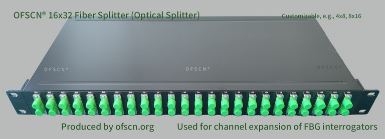
Main Technical Specifications
- Standard Configurations: Commonly include 16 \times 32 splitters, 8 \times 16 splitters, 4 \times 8 splitters, 32 \times 64 splitters, etc.
- Temperature Resistance Customization: Products are designed for standard operating temperatures by default. High-temperature splitters capable of withstanding temperatures up to 250^\circ\text{C} can be customized for special industrial environments.
Innovative Applications in Fiber Bragg Grating Interrogation Systems
In large-scale fiber optic sensing projects, OFSCN® optical splitters are primarily used as “physical channel expansion devices” in conjunction with the OFSCN® Fiber Bragg Grating Interrogator:
- System Architecture Reuse: Through strict and scientific wavelength planning, a single physical channel of the interrogator can be logically expanded into two or three physical branches (while still being processed as a single channel internally by the interrogator).
- Application Advantages: This usage scheme significantly increases the number of Fiber Bragg Grating (FBG) sensor measurement points that can be connected to a single interrogator without compromising the system’s high sampling frequency and wavelength resolution. It substantially reduces the hardware channel cost per measurement point in large-scale engineering projects.